PCB Lab Manufacturer,Supplier and Exporter in India
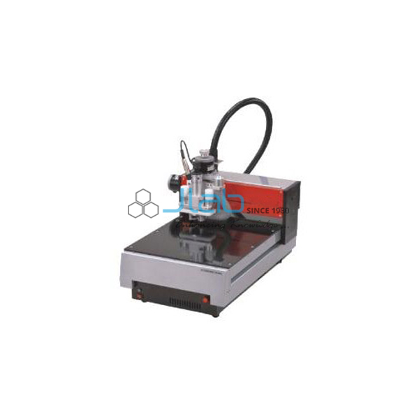
Product Code : JL-PFS-10406
Jlab Export is a leading PCB Lab Manufacturer,and suppliers in India

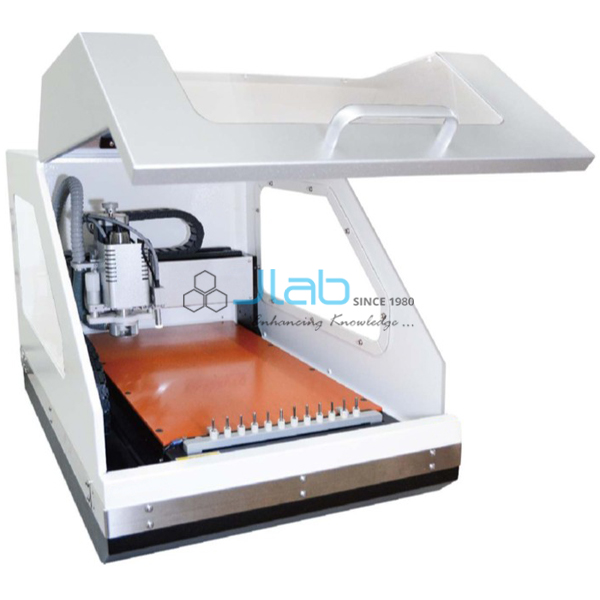
Product Code : JL-PFS-10406
Jlab Export is a leading PCB Lab Manufacturer,and suppliers in India
©2026 Jain Laboratory Instruments PVT.LTD. All Right Reserved
Jlab Export has regular exports of Lab Glassware Manufacturer in India , Educational Scientific Instruments, School Laboratory Scientific Equipment , Biology Lab Equipment ,Physics Lab Equipment , Chemistry Lab Instruments , Laboratory Equipment , Biology Lab Equipment , School lab , Math Lab , Electronics Lab Trainer, Microscopes , Engineering Lab Equipment and Petroleum Testing Equipment, Survey Instruments, Hospital Equipment, Medical Monitoring System and Physiotherapy Equipment for Schools, Colleges, University & Research Labs. for the following countries: India, Afghanistan, Albania, Algeria, Andorra, Angola, Antigua and Barbuda, Argentina, Armenia, Australia, Austria, Azerbaijan, Bahamas, Bahrain, Bangladesh, Barbados, Belarus, Belgium, Belize, Benin, Bhutan, Bolivia, Bosnia and Herzegovina, Botswana, Brazil, Brunei, Bulgaria, Burkina Faso, Burma/ Myanmar, Burundi, Cambodia, Cameroon, Canada, Cape Verde, Central African Republic, Chad, Chile, Colombia, Comoros, Congo, Congo, Costa Rica, Cote d'Ivoire/Ivory Coast, Croatia, Cuba, Cyprus, Czech Republic, Denmark, Djibouti, Dominica, Dominican Republic, East Timor, Ecuador, Egypt, El Salvador, Equatorial Guinea, Eritrea, Estonia, Ethiopia (Addis Ababa), Fiji, Finland, France, Gabon, Gambia, Georgia, Germany, Ghana, Greece, Grenada, Guatemala, Guinea, Guinea-Bissau, Guyana, Haiti, Honduras, Hungary, Iceland, Indonesia, Iran, Iraq, Ireland, Israel, Italy, Jamaica, Japan, Jordan, Kazakstan, Kenya (Nairobi), Kiribati, Korea, North, Korea, South, Kuwait, Kyrgyzstan, Laos, Latvia, Lebanon, Lesotho, Liberia, Liechtenstein, Lithuania, Luxembourg, Macedonia, Madagascar, Malawi (Lilongwe), Malaysia (Kuala Lumpur), Maldives, Mali, Malta, Marshall Islands, Mauritania, Mauritius, Mexico, Micronesia, Moldova, Monaco, Mongolia, Montenegro, Morocco, Mozambique, Namibia, Nauru, Nepal, Netherlands, New Zealand, Nicaragua, Niger, Nigeria (Abuja), Norway, Oman, Palau, Panama, Papua New Guinea, Paraguay, Peru, Philippines (Manila), Poland, Portugal, Qatar, Romania, Russia, Rwanda (Kigali), Saint Kitts and Nevis, Saint Lucia, Saint Vincent and the Grenadines, Samoa, San Marino, Sao Tome and Principe, Saudi Arabia, Senegal, Serbia, Seychelles, Sierra Leone, Singapore, Slovakia, Slovenia, Solomon Islands, Somalia, South Africa, South Sudan, Spain, Sri Lanka, Sudan, Suriname, Swaziland, Sweden, Switzerland, Syria, Tajikistan, Tanzania, Thailand, Togo, Tonga, Trinidad and Tobago, Tunisia, Turkey, Turkmenistan, Tuvalu, Uganda (Kampala), Ukraine, United Arab Emirates (Dubai), United Kingdom (London), United States, Uruguay, Uzbekistan, Vanuatu, Venezuela, Vietnam, Yemen , Zambia (Lusaka), Zimbabwe