
PCB Proto System Manufacturer,Supplier and Exporter in India
Product Code : EL-FOT-10293
Jlab Export is a leading PCB Proto System Manufacturer,and suppliers in India
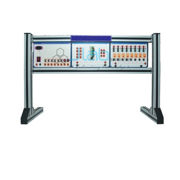
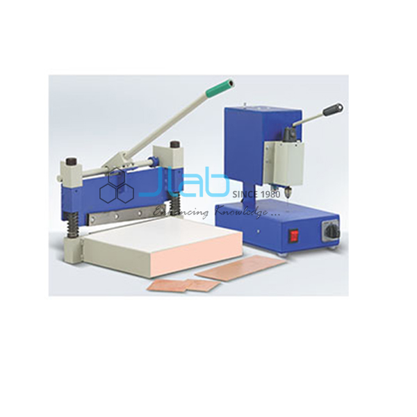
PCB Proto System (code EL-FOT-10293) is a set of machines for making printed circuit board prototypes by the photoresist route, running from PCB layout software and an artwork film maker to etching, drilling, shearing and roller tinning. The system’s machines are made by Jain Laboratory Instruments Pvt Ltd (JLab) at its works in Ambala, India.
Specifications
| Parameter | Detail |
|---|---|
| Machines | PCB artwork film maker; photo resist dip coating machine; double-sided UV exposure unit; dye/developer machine; etching machine; PCB curing machine (oven); PCB drilling machine; PCB shearing machine; roller tinning machine |
| Software | PCB layout software |
| Quality check | Each system is visually inspected before dispatch |
| Pack quantity | Each (sold individually) |
| Minimum order quantity | 10 units |
| Dispatch time | Usually 7–10 working days |
| Product code | EL-FOT-10293 |
| Manufacturer | Jain Laboratory Instruments Pvt Ltd (JLab) — OEM |
| Country of origin | India (made in Ambala, Haryana) |
What Is the PCB Proto System Used For?
It is used to turn a circuit design into a working board in-house. In the photoresist route the layout becomes an artwork film, UV light transfers that pattern onto a photoresist-coated board, and etching removes the unprotected copper so that only the circuit tracks remain.
Frequently Asked Questions
How does the photoresist method differ from screen printing?
The photoresist method transfers the circuit photographically onto a light-sensitive coating on the board, which suits fine tracks and one-off prototypes; screen printing pushes resist ink through a patterned screen and suits repeated boards of the same design.
What does the roller tinning machine do?
It coats the copper tracks with a thin layer of tin, which protects them from oxidation and makes soldering easier.
Who manufactures the PCB Proto System?
JLab makes the system’s machines at its own works in Ambala, Haryana.
OEM Manufacturer
JLab is the trading name of Jain Laboratory Instruments Pvt Ltd, a maker of electronic lab instruments and engineering lab equipment in India, incorporated in 2017 and based on Hargolal Road, Ambala, Haryana. Its machines are built in its own works rather than bought from a trader, so institutes, dealers and importers buy factory-direct, with repeat orders and spares from the same source. JLab exports worldwide and ships to buyers in every region — for example the Netherlands in Western Europe, South Africa in Southern Africa, Malaysia in Southeast Asia, Hong Kong in East Asia and Uganda in East Africa. Tender buyers will find details on the JLab lab tenders page.
Other PCB Fabrication Systems
- PCB Design and Fabrication Lab — a photoresist-route PCB lab with a PCB design kit and an artwork table.
- PCB Lab — makes boards by the screen printing method.
- PCB Prototyping System — a machine that produces a PCB prototype from a Gerber file.
Compare them in the PCB Fabrication Systems range, or browse Electronics Lab Equipments.
Request a Quote
Request a quotation through the Add To Cart button or the contact page, stating how many systems you need, the destination country and port, and your delivery terms (for example FOB or CIF).
Last updated: 22 October 2026