
FET Characteristics Apparatus Manufacturer,Supplier and Exporter in India
Product Code : EL-SCD-1081
Jlab Export is a leading FET Characteristics Apparatus Manufacturer,and suppliers in India
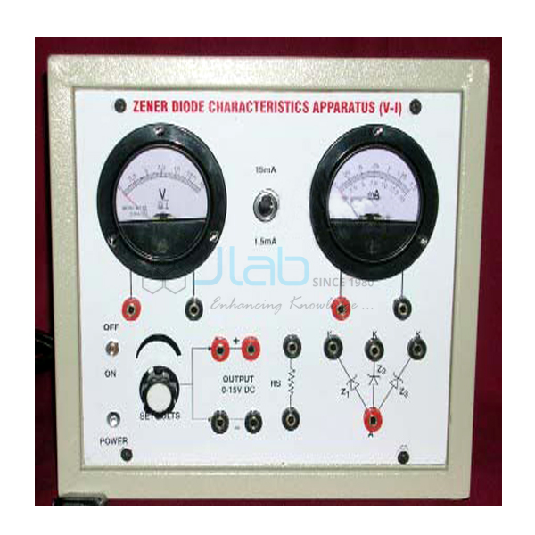
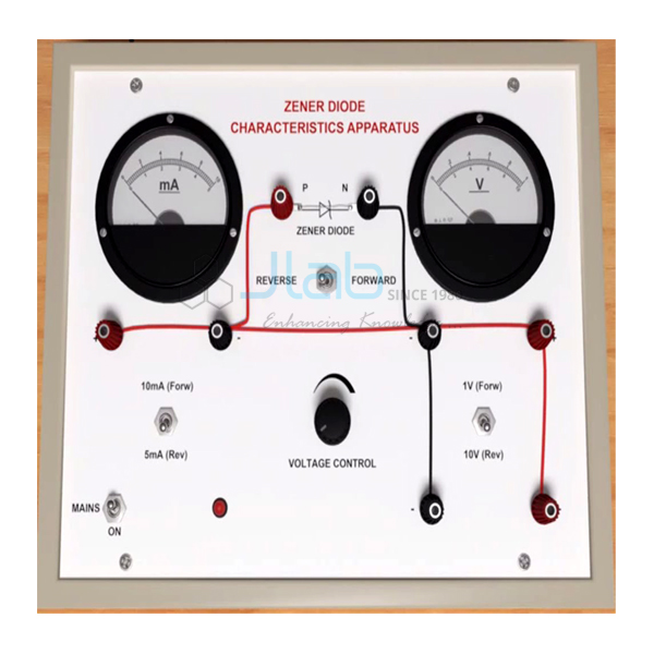
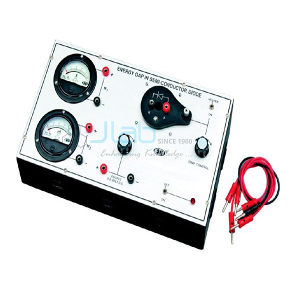
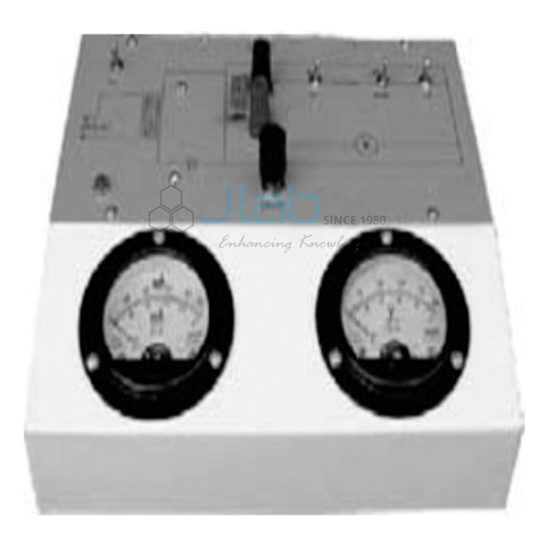
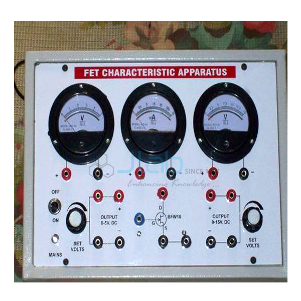
FET Characteristics Apparatus (code EL-SCD-1081) is a bench unit for plotting the static (drain) and transfer characteristics of a field-effect transistor, using a BFW10 FET mounted on the panel. Two DC regulated power supplies, 0–10 V DC/10 mA and 0–5 V DC, and three meters for voltage and current are wired to terminals in an 11 x 8 x 4 inch unit. It is made by Jain Laboratory Instruments Pvt Ltd (JLab) at its works in Ambala, India.
Specifications
| Parameter | Detail |
|---|---|
| Experiments | Static and transfer characteristics of a FET |
| Device | FET type BFW10, mounted on the panel |
| DC regulated power supplies | Two: 0–10 V DC/10 mA and 0–5 V DC |
| Meters | Three, for voltage and current measurement |
| Connections | Supplies, meters and FET brought out on terminals |
| Dimensions | 11 x 8 x 4 in (about 28 x 20 x 10 cm) |
| Quality check | Each apparatus is visually inspected before dispatch |
| Pack quantity | Each (sold individually) |
| Minimum order quantity | 10 units |
| Dispatch time | Usually 7–10 working days |
| Product code | EL-SCD-1081 |
| Manufacturer | Jain Laboratory Instruments Pvt Ltd (JLab) — OEM |
| Country of origin | India (made in Ambala, Haryana) |
How Does It Compare with the JLab MOSFET Apparatus?
| Model | Device | Characteristics (as listed) | Supplies and meters |
|---|---|---|---|
| This apparatus (EL-SCD-1081) | FET type BFW10 | Static (drain) and transfer | 0–10 V DC/10 mA and 0–5 V DC; three meters |
| Mosfet Characteristics Apparatus | MOSFET | Drain characteristics for different gate–source voltages | 0–10 V DC, 10 mA and 0–5 V DC; three meters |
Choose this apparatus to teach the junction FET with both of its characteristic curves. The MOSFET apparatus has the same supply and meter arrangement for labs that also cover the insulated-gate device.
What Is the FET Characteristics Apparatus Used For?
The BFW10 is an n-channel junction FET, a device in which the gate voltage, not a base current, controls the drain current. For the static or drain characteristic, students hold the gate–source voltage fixed and plot drain current against drain–source voltage, then repeat for a few gate voltages; each curve rises through the ohmic region and flattens beyond pinch-off into the saturation region. For the transfer characteristic, they hold the drain–source voltage fixed and plot drain current against gate–source voltage, from the maximum drain current at zero gate voltage down towards cut-off as the gate is made more negative. From the curves they work out the transconductance, the drain resistance and the amplification factor (their product), the figures used later when designing a common source amplifier.
Because the gate junction is reverse-biased, the FET draws almost no gate current and has a very high input resistance. The apparatus serves B.Sc. physics and electronics practicals, electronic devices labs in engineering and polytechnic courses, and ITI electronics training. Keep the gate reverse-biased, increase the drain voltage gradually and switch off before changing connections.
What to Specify When Ordering
- Spare FETs — order spare BFW10 devices for student use.
- Meter ranges — not given in the listing; ask JLab if your worksheet needs particular ranges.
- Quantity — the minimum order is 10 units.
Frequently Asked Questions
Which FET is fitted?
A BFW10, mounted on the panel with its connections on terminals. The BFW10 is an n-channel junction FET.
Which characteristics can be plotted?
The static (drain) characteristics and the transfer characteristic, from which transconductance, drain resistance and amplification factor are calculated.
What supplies and meters does it have?
Two DC regulated supplies, 0–10 V DC/10 mA and 0–5 V DC, and three meters for voltage and current.
Is this the same as the MOSFET apparatus?
No. This unit uses a junction FET; the Mosfet Characteristics Apparatus uses a MOSFET and is listed for drain characteristics.
Who manufactures this apparatus?
Jain Laboratory Instruments Pvt Ltd (JLab), at its works in Ambala, Haryana, India.
OEM Manufacturer
JLab is the trading name of Jain Laboratory Instruments Pvt Ltd, an electronic lab instruments manufacturer in India, incorporated in 2017 and based on Hargolal Road, Ambala, Haryana. The FET apparatus is built at JLab’s own works, not resold from a trader, so colleges, institutes, dealers and importers order it straight from the maker; each unit is visually inspected before dispatch, and repeat orders and spare devices are handled at the works. JLab exports worldwide and ships to buyers in every region — for example Ivory Coast in West Africa, the Dominican Republic in Central America and the Caribbean, New Zealand in Oceania, Mexico in North America and Belgium in Western Europe. Tender details are on the JLab lab tenders page.
Related Transistor and FET Apparatus
- Mosfet Characteristics Apparatus — drain characteristics of a MOSFET with a matching supply arrangement.
- FET Common Source Amplifier — voltage gain and frequency response of a FET amplifier, the next experiment.
- Transistor Characteristics Apparatus — the bipolar transistor counterpart, in common base and common emitter.
See the full Semi Conductor Devices range or all Scientific Instrument apparatus.
Request a Quote
Quotes come direct from the manufacturer. Use the Add To Cart enquiry button, or send the quantity (minimum 10 units), the number of spare FETs and your delivery location through the contact page.
Last updated: 9 October 2026