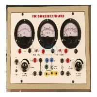

Semi Conductor Devices Manufacturer, Suppliers and Exporter in India
Jlabexport is a leading Semi Conductor Devices Manufacturer,and suppliers in India, United States, Indonesia, Brazil, Bangladesh, Mexico, Japan, Egypt, Philippines, Democratic Republic of the Congo, Vietnam, Iran, Turkey, Tanzania, United Kingdom, France, South Africa, Italy, Kenya, Colombia, Sudan, Uganda, South Korea, Argentina, Afghanistan, Yemen, Angola, Morocco, Poland, Uzbekistan, Mozambique, Malaysia, Ghana, Saudi Arabia, Peru, Madagascar, Côte d’Ivoire, Cameroon, Niger, Venezuela, Australia, Syria, Mali, Burkina Faso, Sri Lanka, Malawi, Zambia, Chad, Kazakhstan, Somalia, Chile, Senegal, Ecuador, Cambodia, Zimbabwe, Guinea, Benin, Rwanda, Burundi, Bolivia, South Sudan, Tunisia, Haiti, Belgium, Dominican Republic, Jordan, United Arab Emirates, Honduras, Tajikistan, Papua New Guinea, Portugal, Togo, Sierra Leone, Belarus, Laos, Turkmenistan, Libya, Kyrgyzstan, Nicaragua, Paraguay, Bulgaria, Serbia, Republic of the Congo, Lebanon, Liberia, Central African Republic, Palestine, Oman, Mauritania, New Zealand, Costa Rica, Kuwait, Panama, Croatia, Georgia, Eritrea, Mongolia, Uruguay, Qatar, Namibia, Bosnia and Herzegovina, Moldova, Armenia, Gambia, Jamaica, Lithuania, Albania, Gabon, Botswana, Lesotho, Guinea-Bissau, Slovenia, Equatorial Guinea, Latvia, North Macedonia, Bahrain, Trinidad and Tobago, Timor-Leste, Cyprus, Estonia, Eswatini, Mauritius, Djibouti, Fiji, Comoros, Solomon Islands, Guyana, Bhutan, Luxembourg, Suriname, Montenegro, Malta, Maldives, Cabo Verde, Brunei, Belize, Bahamas, Iceland, Vanuatu, Barbados, São Tomé and Príncipe, Samoa, Saint Lucia, Kiribati, Seychelles, Grenada, Saint Vincent and the Grenadines, Antigua and Barbuda.
Last updated: 22 October 2026
Quick Answer
Semi Conductor Devices is a range of panel apparatus for semiconductor practicals in physics and electronics laboratories, most with their own DC power supply, meters and a mounted device brought out on terminals. It covers PN junction and zener diode characteristics, the energy band gap, transistor and FET characteristics, h-parameters, and SCR, diac, triac and UJT studies, plus ultrasonic velocity and dielectric constant set-ups. JLab currently lists 14 items in this category.
Request a quotation | Jump to the product list
Explore the Semi Conductor Devices Range
| Range | Items | What it covers |
|---|---|---|
| Diode and Zener Diode Apparatus | 5 | Forward and reverse characteristics of PN junction and zener diodes, zener voltage stabilization against input and load, and the energy band gap from reverse saturation current in a diode oven. |
| Transistor and FET Apparatus | 3 | PNP and NPN transistor characteristics with four meters, h-parameters of a PNP transistor in common emitter, and static and transfer characteristics of a BFW10 FET. |
| SCR, Diac, Triac and Thyristor Apparatus | 4 | SCR anode characteristics with a 0-150 V DC supply, diac V-I and triac MT characteristics, and a thyristor panel with UJT, SCR, diac and triac and three regulated supplies. |
| Ultrasonic and Dielectric Experiments | 2 | Velocity of ultrasonic waves with a 3-8 MHz RF oscillator, crystal tank and spectrometer, and dielectric constant of liquids and solids with a tunable high-frequency oscillator. |
Semi Conductor Devices Specifications
The tables list the experiment, regulated supplies, meters and panel size stated for each apparatus, grouped by diode, transistor, thyristor and other set-ups.
Diode and Zener Diode Apparatus (5)
| Product | Specification |
|---|---|
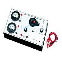
| Semiconductor Diode and PN Junction Diode Apparatus | Experiment: Forward and reverse characteristics of a PN junction diode; DC power supplies: Two: 0–50 V, 2 mA and 0–1 V, 200 mA; Dimensions: 10 x 8 x 4 in (about 25 x 20 x 10 cm). |
| Voltage Stabilization Characteristics of Zener Diode | Experiments: Input voltage versus output voltage characteristic; output voltage versus load characteristic; Meters: Two round meters, for input voltage and output voltage; Dimensions: 10 x 8 x 4 in (about 25 x 20 x 10 cm). |
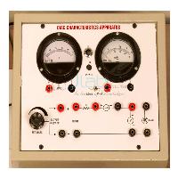
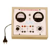
| Zener Diode Characteristics Apparatus Forward and Reverse V-I Characteristics | Experiment: Forward and reverse V–I characteristics of a zener diode; DC regulated power supply: 0–25 V DC, 15 mA; Dimensions: 10 x 8 x 4 in (about 25 x 20 x 10 cm). |
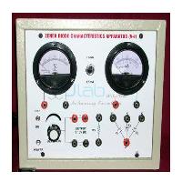
| PN Junction and Zener Diode Characteristics Apparatus Forward and Reverse V-I Characteristics | Experiments: Forward and reverse characteristics of a PN junction diode and of a zener diode; Meters: Two double-range meters, for voltage and current; Dimensions: 15 x 8 x 4 in (about 38 x 20 x 10 cm). |
| Energy Band Gap of PN Junction Diode | Experiment: Reverse saturation current versus temperature in a reverse-biased PN junction diode; Diode: One PN junction diode, placed in an oven; Temperature: Thermometer reading to 100 °C; temperature control system. |
Transistor and FET Apparatus (3)
| Product | Specification |
|---|---|
| H Parameters of PNP Transistor in Common Emitter Model | Experiment: Calculation of h-parameters such as current gain, input impedance and output impedance; Transistor: One PNP transistor, mounted; common emitter configuration; DC regulated power supplies: Two: 0–10 V DC, 500 mA/50 mA; and 0–1 V DC at 30 mA. |
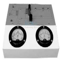
| Transistor Characteristics Apparatus | Transistors: One PNP and one NPN, mounted behind the panel; DC regulated power supplies: Two: 0–10 V DC/500 mA/50 mA and 0–1 V DC/30 mA; Meters: Four round meters for voltage and current measurement. |
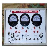
| FET Characteristics Apparatus | Experiments: Static and transfer characteristics of a FET; Device: FET type BFW10, mounted on the panel; DC regulated power supplies: Two: 0–10 V DC/10 mA and 0–5 V DC. |
SCR, Diac, Triac and Thyristor Apparatus (4)
| Product | Specification |
|---|---|
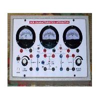
| SCR Characteristics Apparatus | Experiment: Anode current versus anode–cathode voltage characteristic of an SCR; DC regulated power supplies: Two: 0–3 V DC/50 mA and 0–150 V DC; Meters: Three, for voltage and current measurement. |
| Characteristics and Applications Thyristors | Experiments: Characteristics and applications of the diac, triac, UJT and SCR; DC regulated power supplies: Three: 0–15 V DC/150 mA; 0–50 V DC/100 mA; 0–2.5 V DC/200 mA; Meters: Four dual-range meters, for voltage and current measurement. |
| Diac Characteristics Apparatus | Experiment: To study the V–I characteristics of a diac; Power supply: DC regulated, 0–50 V DC / 100 mA; Dimensions: 15 x 8 x 4 in (about 38 x 20 x 10 cm). |
| Triac Characteristics Apparatus | Experiment: MT characteristics of a triac with gate signal; Power supplies: Two DC regulated supplies: 0–25 V DC / 100 mA and 0–5 V DC / 200 mA; Meters: Three round meters for voltage and current measurement. |
Ultrasonic and Dielectric Experiments (2)
| Product | Specification |
|---|---|
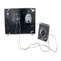
| Ultrasonic Diffraction Grating Experiment | Experiment: Determination of the velocity of ultrasonic waves; RF oscillator: 3–8 MHz; Spectrometer: 9 in (about 23 cm) bed. |
| Dielectric Constant Apparatus | Experiment: Calculation of the dielectric constant of liquids and solids; Oscillator: High-frequency oscillator, tunable; Sample position: Between parallel plates. |
Who Buys This Range
Physics and electronics laboratories of colleges, polytechnics and engineering institutes that teach device characteristics with the diode, zener, transistor, FET, SCR, diac and triac panels, and degree-level physics practicals on the energy band gap, ultrasonic velocity and dielectric constant.
Frequently Asked Questions
Which thyristor devices can be studied with this range?
The SCR Characteristics Apparatus plots anode current against anode-cathode voltage, the diac and triac apparatus give the V-I and MT characteristics of a diac and a triac, and the Characteristics and Applications Thyristors panel covers the diac, triac, UJT and SCR with three regulated supplies and four dual-range meters.
How is the energy band gap of a PN junction diode measured with this apparatus?
The Energy Band Gap of PN Junction Diode apparatus places a reverse-biased PN junction diode in an oven with a temperature control system and a thermometer reading to 100 °C, and two meters record the reverse saturation current as the temperature changes.
Request a Quote
Name the apparatus and how many sets you need, for example the Transistor Characteristics Apparatus or the Energy Band Gap of PN Junction Diode, and send the request from the contact page.
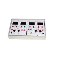
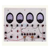
Transistor Characteristics Apparatus
Product Code : EL-SCD-1079
Input and output characteristics of PNP and NPN transistors in common base and common emitter configurations.
View Details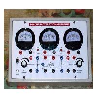
Zener Diode Characteristics Apparatus Forward and Reverse V-I Characteristics
Product Code : EL-SCD-1084
View Details
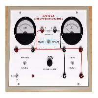
PN Junction and Zener Diode Characteristics Apparatus Forward and Reverse V-I Characteristics
Product Code : EL-SCD-1085
View Details