
Semiconductor Diode and PN Junction Diode Apparatus Manufacturer,Supplier and Exporter in India
Product Code : EL-SCD-1082
Jlab Export is a leading Semiconductor Diode and PN Junction Diode Apparatus Manufacturer,and suppliers in India
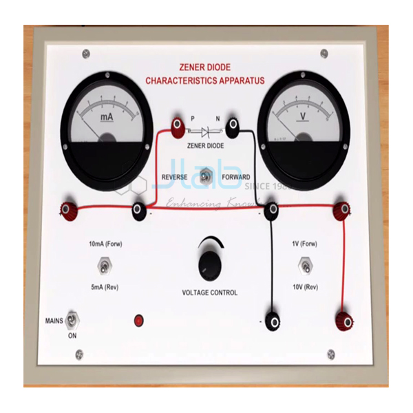
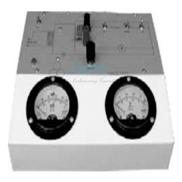
Semiconductor Diode and PN Junction Diode Apparatus (code EL-SCD-1082) is a semiconductor diode kit for physics labs, used to plot the forward and reverse characteristics of a PN junction diode in school, college and technical-course practicals. It has two DC power supplies, 0–50 V at 2 mA and 0–1 V at 200 mA, two meters and mounted PN junction diodes, all connected through terminals. It is made by Jain Laboratory Instruments Pvt Ltd (JLab) at its works in Ambala, India.
Specifications
| Parameter | Detail |
|---|---|
| Experiment | Forward and reverse characteristics of a PN junction diode |
| DC power supplies | Two: 0–50 V, 2 mA and 0–1 V, 200 mA |
| Meters | Two, for voltage and current measurement |
| Diodes | PN junction diodes, mounted |
| Connections | Supplies, meters and diodes brought out on terminals |
| Dimensions | 10 x 8 x 4 in (about 25 x 20 x 10 cm) |
| Quality check | Each apparatus is visually inspected before dispatch |
| Pack quantity | Each (sold individually) |
| Minimum order quantity | 10 units |
| Dispatch time | Usually 7–10 working days |
| Product code | EL-SCD-1082 |
| Manufacturer | Jain Laboratory Instruments Pvt Ltd (JLab) — OEM |
| Country of origin | India (made in Ambala, Haryana) |
How Does It Compare with Other JLab Diode Apparatus?
| Model | Diodes studied | Supplies and meters (as listed) |
|---|---|---|
| This apparatus (EL-SCD-1082) | PN junction diode, forward and reverse | Two DC supplies (0–50 V, 2 mA and 0–1 V, 200 mA); two meters |
| PN Junction and Zener Diode Characteristics Apparatus | PN junction diode and zener diode, forward and reverse | Two DC supplies; two double-range meters |
| Semiconductor Diode | Germanium and silicon diodes, forward and reverse; static and dynamic resistance | One continuously variable regulated supply with coarse and fine controls; digital voltmeter and current meter |
Choose this apparatus for the basic PN junction experiment with separate supplies for the forward and reverse runs. The PN junction and zener model adds the zener diode in one unit, and the semiconductor diode board compares germanium with silicon on digital meters.
What Is the PN Junction Diode Apparatus Used For?
A PN junction conducts easily in one direction only. In forward bias the current stays very small until the applied voltage passes the knee (cut-in) voltage and then rises steeply; in reverse bias only a tiny reverse saturation current flows until breakdown. The listed supplies match these two regions: the 0–1 V, 200 mA supply suits the forward run, where small voltage steps give large current changes, and the 0–50 V, 2 mA supply suits the reverse run, where the voltage is larger and the current very small. Students plot current against voltage for both directions, read off the knee voltage, and calculate the static resistance (voltage divided by current) and the dynamic resistance (change in voltage divided by change in current) of the forward-biased junction.
Drawing the I–V characteristic of a p-n junction diode in forward and reverse bias is one of the class 12 physics practicals, and the same experiment opens semiconductor work in B.Sc. physics and electronics, diploma and ITI labs; its curves explain the rectifier, clipper and zener regulator circuits that follow. Raise the voltage slowly, use the low-voltage supply for the forward run, and switch off before changing connections on the terminals.
What to Specify When Ordering
- Diode types and spares — the listing does not name the diodes fitted; ask for the types and order spares.
- Meter ranges — request them if your worksheet uses fixed ranges.
- Quantity — the minimum order is 10 units.
Frequently Asked Questions
What does this apparatus measure?
The forward and reverse characteristics of a PN junction diode: current against voltage in both bias directions, read on the two meters.
Why does it have two power supplies?
The forward and reverse regions need very different ranges. The 0–1 V, 200 mA supply suits the forward run, and the 0–50 V, 2 mA supply suits the reverse run.
Is it suitable for the class 12 diode practical?
Yes. It covers the I–V characteristic of a p-n junction diode in forward and reverse bias, which is the class 12 physics practical, and it is equally used in college labs.
Does it include a zener diode?
No, this listing covers PN junction diodes. For PN junction and zener diodes in one unit, see the PN Junction and Zener Diode Characteristics Apparatus.
Who manufactures this apparatus?
Jain Laboratory Instruments Pvt Ltd, trading as JLab, makes it at its works in Ambala, Haryana, India.
OEM Manufacturer
JLab is the trading name of Jain Laboratory Instruments Pvt Ltd, a physics and electronics lab equipment manufacturer in India, incorporated in 2017 and based on Hargolal Road, Ambala, Haryana. The diode apparatus is assembled in JLab’s own works rather than bought from a trader, so schools, colleges, dealers and importers buy it factory-direct; every unit is visually inspected before dispatch, and repeat orders and spare diodes are handled by the manufacturer. JLab exports worldwide and ships to buyers in every region — for example Ghana in West Africa, Gabon in Central Africa, the Maldives in South Asia, Japan in East Asia and Tanzania in East Africa. Tender buyers can refer to the JLab lab tenders page.
Related Diode Apparatus
- PN Junction and Zener Diode Characteristics Apparatus — both diode types, forward and reverse, in one unit.
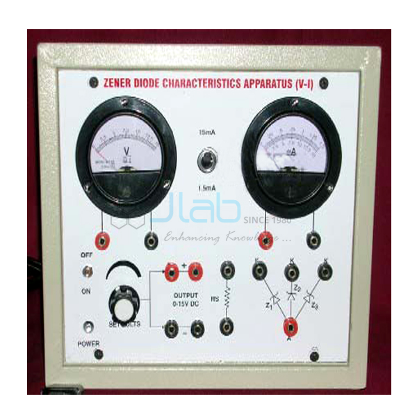
- Zener Diode Characteristics Apparatus — forward and reverse V–I characteristics of zener diodes.
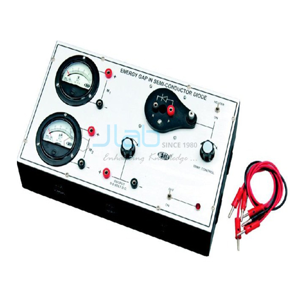
- Energy Band Gap of PN Junction Diode — reverse saturation current against temperature to find the band gap.
- Half Wave, Full Wave and Rectifier Apparatus — the diode put to work in rectifier circuits.
- Clipping and Clamping Circuit Apparatus — diode wave-shaping circuits.
See the full Semi Conductor Devices range or all Scientific Instrument apparatus.
Request a Quote
Quotes come direct from the manufacturer. Use the Add To Cart enquiry button, or send the quantity (minimum 10 units), any spare diodes and your delivery location through the contact page.
Last updated: 9 October 2026