
H Parameters of PNP Transistor in Common Emitter Model Manufacturer,Supplier and Exporter in India
Product Code : EL-SCD-1078
Jlab Export is a leading H Parameters of PNP Transistor in Common Emitter Model Manufacturer,and suppliers in India
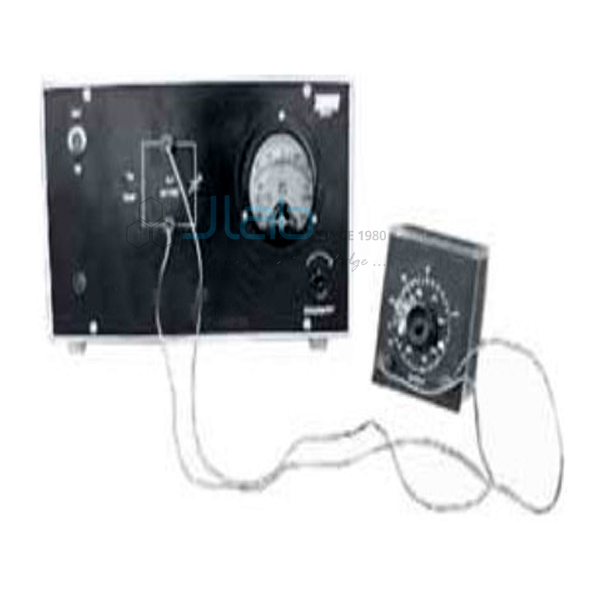
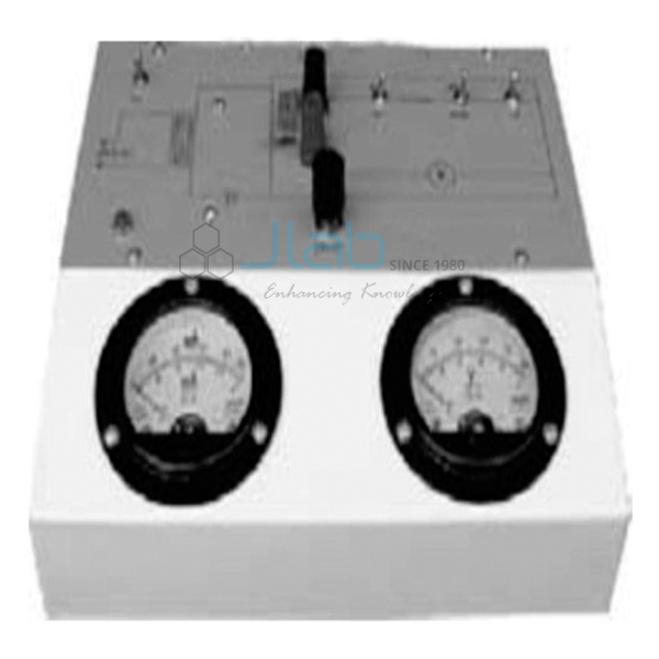
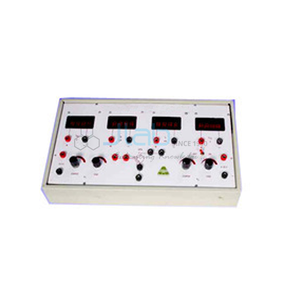
H Parameters of PNP Transistor in Common Emitter Model (code EL-SCD-1078) is a bench apparatus for finding the hybrid (h) parameters of a PNP transistor connected in common emitter mode — current gain, input impedance and output impedance — in electronics and physics labs. It has two DC regulated power supplies, four meters and a mounted PNP transistor, with all connections on terminals. It is made by Jain Laboratory Instruments Pvt Ltd (JLab) at its works in Ambala, India.
Get a quote: use the Add To Cart enquiry button below, or send your quantity and destination through the contact page.
Specifications
| Parameter | Detail |
|---|---|
| Experiment | Calculation of h-parameters such as current gain, input impedance and output impedance |
| Transistor | One PNP transistor, mounted; common emitter configuration |
| DC regulated power supplies | Two: 0–10 V DC, 500 mA/50 mA; and 0–1 V DC at 30 mA |
| Meters | Four |
| Connections | Supplies, meters and transistor connected on terminals |
| Also mentioned in the listing | Oscillator (details to be confirmed with JLab) |
| Quality check | Each apparatus is visually inspected before dispatch |
| Pack quantity | Each (sold individually) |
| Minimum order quantity | 10 units |
| Dispatch time | Usually 7–10 working days |
| Product code | EL-SCD-1078 |
| Manufacturer | Jain Laboratory Instruments Pvt Ltd (JLab) — OEM |
| Country of origin | India (made in Ambala, Haryana) |
What Is the H-Parameter Apparatus Used For?
The h-parameter, or hybrid, model describes a transistor for small signals with four numbers. In common emitter mode they are the input impedance hie (change in base–emitter voltage divided by change in base current, at constant collector–emitter voltage), the forward current gain hfe (change in collector current divided by change in base current, at constant collector–emitter voltage), the reverse voltage ratio hre and the output admittance hoe, whose reciprocal is the output impedance. Students set the operating point from the two supplies, record voltages and currents on the four meters, plot the input and output characteristics, and read the parameters from the slopes of the curves. Because this is a PNP device, the collector and base are negative with respect to the emitter, the reverse of an NPN set-up.
The h-parameters feed straight into small-signal amplifier calculations, which is why the experiment is a regular part of B.Sc. physics and electronics practicals and of electronic devices and circuits labs in engineering and polytechnic courses. Raise both supplies slowly from zero, keep the collector current within the transistor’s rating, and switch off before changing any connection on the terminals.
What to Specify When Ordering
- Oscillator — the listing mentions an oscillator; confirm whether it is supplied with the apparatus and how it is used.
- Transistor type and spares — the PNP transistor type is not named; ask for it and order spare transistors for student use.
- Size — ask JLab for the cabinet dimensions if bench space is limited.
- Quantity — the minimum order is 10 units.
Frequently Asked Questions
Which h-parameters can be determined?
The listing names current gain, input impedance and output impedance. The reverse voltage ratio can also be estimated from input curves taken at two collector voltages.
What power supplies are built in?
Two DC regulated supplies: 0–10 V DC, 500 mA/50 mA, and 0–1 V DC at 30 mA, with their connections on terminals.
Can it test NPN transistors as well?
This apparatus is listed with one PNP transistor. For input and output characteristics of both PNP and NPN transistors, see the Transistor Characteristics Apparatus linked below.
Is an oscillator included?
The listing mentions an oscillator but gives no details. Ask JLab to confirm before ordering if your method needs an AC signal source.
What is the minimum order and dispatch time?
The minimum order is 10 units, and orders usually leave within 7–10 working days after visual inspection. Export transit time depends on the destination.
Who manufactures this apparatus?
Jain Laboratory Instruments Pvt Ltd, trading as JLab, makes it at its works in Ambala, Haryana, India.
OEM Manufacturer
JLab is the trading name of Jain Laboratory Instruments Pvt Ltd, an electronics and physics teaching equipment manufacturer in India, incorporated in 2017 and based on Hargolal Road, Ambala, Haryana. This h-parameter apparatus is wired and assembled in JLab’s own works, not purchased from a trader, so colleges, institutes, dealers and importers buy it at source; each unit is visually inspected before dispatch, and repeat orders and spare transistors are handled by the manufacturer. JLab exports worldwide and ships to buyers in every region — for example Namibia in Southern Africa, Taiwan in East Asia, Zimbabwe in East Africa, Chad in Central Africa and Qatar in the Middle East. For tender enquiries, visit the JLab lab tenders page.
Related Transistor Apparatus
- Transistor Characteristics Apparatus — input and output characteristics of PNP and NPN transistors in common base and common emitter.
- Biasing of Transistor BJT — compares fixed, collector-to-base, emitter resistor and voltage divider bias.
- Study of Transistor Amplifier Circuits — frequency response and input and output impedance of transistor amplifiers.
- FET Characteristics Apparatus — static and transfer characteristics of a field-effect transistor.
See the full Semi Conductor Devices range or all Scientific Instrument apparatus.
Request a Quote
Quotes come direct from the manufacturer. Use the Add To Cart enquiry button, or send the quantity (minimum 10 units), any spare transistors needed and your delivery location through the contact page.
Last updated: 9 October 2026