
Mosfet Characteristics Apparatus Manufacturer,Supplier and Exporter in India
Product Code : EL-SI-1094
Jlab Export is a leading Mosfet Characteristics Apparatus Manufacturer,and suppliers in India
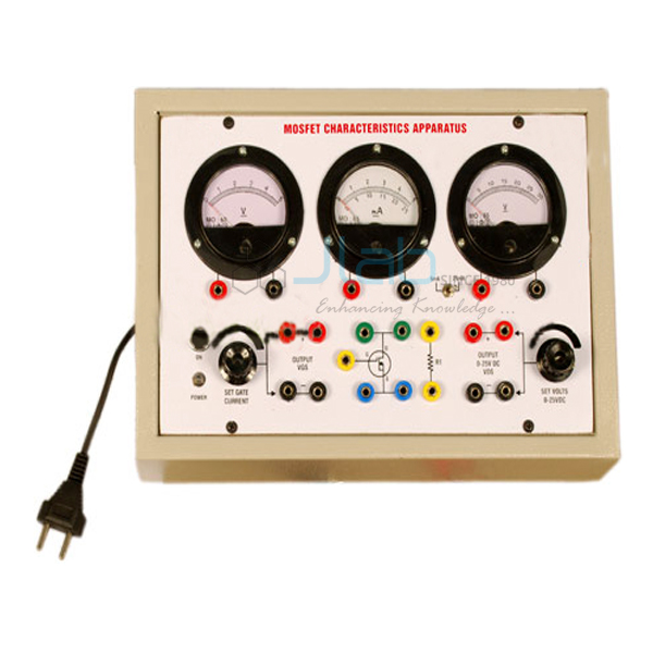
Mosfet Characteristics Apparatus (code EL-SI-1094) is a panel-mounted experiment for plotting the drain characteristics of a MOSFET — drain current against drain–source voltage for different gate–source voltages — in college physics and electronics laboratories. It has two DC power supplies (0–10 V DC, 10 mA and 0–5 V DC), three meters for voltage and current, and a MOSFET mounted on the panel. It is made by Jain Laboratory Instruments Pvt Ltd (JLab) at its works in Ambala, India.
Specifications
| Parameter | Detail |
|---|---|
| Experiment | Drain characteristics: drain current (ID) against drain–source voltage (VDS) for different gate–source voltages (VGS) |
| Power supplies | Two DC supplies: 0–10 V DC, 10 mA and 0–5 V DC |
| Meters | Three, for voltage and current measurement |
| Device under test | One MOSFET, mounted on the panel |
| Dimensions | 11 x 8 x 4 inches |
| Quality check | Each apparatus is visually inspected before dispatch |
| Pack quantity | Each (sold individually) |
| Minimum order quantity | 10 units |
| Dispatch time | Usually 7–10 working days |
| Product code | EL-SI-1094 |
| Manufacturer | Jain Laboratory Instruments Pvt Ltd (JLab) — OEM |
| Country of origin | India (made in Ambala, Haryana) |
How Does It Compare with the JLab FET Characteristics Apparatus?
| Model | Device | Characteristics plotted | Supplies and meters | Size |
|---|---|---|---|---|
| This apparatus (EL-SI-1094) | MOSFET | VDS against ID for different VGS | 0–10 V DC, 10 mA and 0–5 V DC; three meters | 11 x 8 x 4 inches |
| FET Characteristics Apparatus | FET BFW10 (junction FET) | Static and transfer characteristics | Regulated 0–10 V DC, 10 mA and 0–5 V DC; three meters | 11 x 8 x 4 inches |
The two panels share the same supply ranges, meter count and size, so they suit a matched pair of practicals. Choose this apparatus to study an insulated-gate MOSFET, and the FET apparatus to study a junction FET; many colleges order both so students can compare the two device types.
What Is the MOSFET Characteristics Apparatus Used For?
In a MOSFET the gate is insulated from the channel, so the gate–source voltage controls the drain current while the gate itself draws almost no current. Students set a fixed VGS with one supply, raise VDS in steps with the other, record the drain current on the meters, and repeat for several gate voltages. The resulting family of curves shows the ohmic region at low VDS, where current rises roughly in proportion to voltage, and the saturation region, where the drain current levels off and is set mainly by VGS. The same readings show the gate voltage at which the drain current starts to flow, and a graph of ID against VGS gives the transfer characteristic.
The experiment belongs to undergraduate physics and electronics practicals on field-effect devices. Start with both supplies at zero and increase them gradually; because a MOSFET gate is sensitive to static discharge, avoid touching the gate terminal when the panel is not connected.
What to Specify When Ordering
- Quantity — the minimum order is 10 units; plan one for each student group.
- Companion apparatus — the FET, UJT and transistor characteristics apparatus are separate items that complete a semiconductor devices practical set.
- Delivery details — destination country and city or port, delivery terms (for example FOB or CIF) and any tender reference.
Frequently Asked Questions
What does this apparatus measure?
The drain characteristics of a MOSFET: drain current against drain–source voltage, plotted for several values of gate–source voltage.
Which supplies and meters are built in?
Two DC power supplies, 0–10 V DC at 10 mA and 0–5 V DC, and three meters for voltage and current, with the MOSFET mounted on the panel.
How is it different from the FET characteristics apparatus?
Both panels use the same supply ranges, three meters and an 11 x 8 x 4 inch size. This one carries a MOSFET with an insulated gate; the FET apparatus carries a BFW10 junction FET and plots its static and transfer characteristics.
Who manufactures the apparatus?
Jain Laboratory Instruments Pvt Ltd (JLab) makes it at its works in Ambala, Haryana, India, and quotes for it directly.
OEM Manufacturer
JLab is the trading name of Jain Laboratory Instruments Pvt Ltd, a maker of physics and electronics practical apparatus in India, incorporated in 2017 and based on Hargolal Road, Ambala, Haryana. The panel is built in JLab’s own works rather than bought from a trader, so colleges, universities, dealers and importers buy it factory-direct; each unit is visually inspected before dispatch, and repeat orders are handled by the manufacturer. JLab exports worldwide and serves every region — for example Kazakhstan in Central Asia, Norway in Northern Europe, Belize in Central America and the Caribbean, Slovenia in Southern Europe and Liberia in West Africa. Tender information is on the JLab lab tenders page.
Related Semiconductor Device Experiments
- FET Characteristics Apparatus — static and transfer characteristics of a BFW10 junction FET, compared above.
- UJT Characteristics Apparatus — V-I characteristics and interbase resistance of a 2N2646 UJT.
- Transistor Characteristics Apparatus — input and output characteristics of PNP and NPN transistors in common base and common emitter modes.
See the Semi Conductor Devices range, the Scientific Instrument range or the Indian Instruments section.
Request a Quote
Quotes come direct from the manufacturer. Use the Add To Cart enquiry button on this page, or send the number of units (minimum 10), any companion apparatus you need, and your delivery location through the contact page.
Last updated: 8 October 2026