
Transistor Characteristics Apparatus Manufacturer,Supplier and Exporter in India
Product Code : EL-DSO-10321
Jlab Export is a leading Transistor Characteristics Apparatus Manufacturer,and suppliers in India
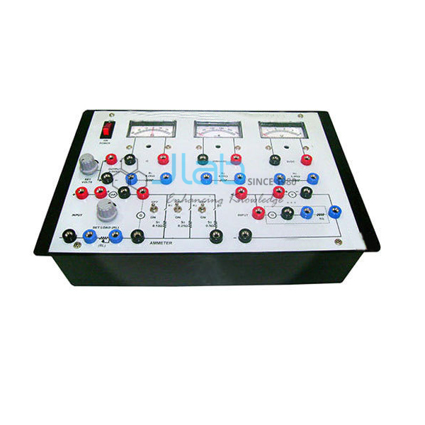
Transistor Characteristics Apparatus (code EL-DSO-10321) is an analog electronics lab apparatus for plotting the input, output and transfer characteristics of a PNP and an NPN transistor in common emitter and common base configurations. Its aluminium front panel carries the symbol diagram, with all important test points brought out. It is made by Jain Laboratory Instruments Pvt Ltd (JLab) at its works in Ambala, India.
Specifications
| Parameter | Detail |
|---|---|
| Objective | Input, output and transfer characteristics of PNP and NPN transistors in common emitter and common base configurations |
| DC regulated power supplies | Inbuilt, variable: 0–1 V DC and 0–10 V DC |
| Meters | On-board analog moving coil meters, 60 x 35 mm |
| Voltmeters | 0–1 V DC; 0–10 V DC |
| Ammeters | 0–50 mA DC; 0–250 µA / 0–50 mA DC (dual range) |
| Transistors provided | PNP: CK 100; NPN: CL 100 |
| Front panel | Aluminium, 300 x 220 mm, symbol diagram printed, all important test points brought out; on a lightweight shock-proof plastic cabinet |
| Power requirement | 230 V AC 10%, 50 Hz |
| Weight | About 2.0 kg |
| Dimensions | 330 (L) x 225 (B) x 75 (H) mm |
| Standard accessories | Power cord, patch cords and instruction manual |
| Quality check | Each apparatus is visually inspected before dispatch |
| Pack quantity | Each (sold individually) |
| Minimum order quantity | 10 units |
| Dispatch time | Usually 7–10 working days |
| Product code | EL-DSO-10321 |
| Manufacturer | Jain Laboratory Instruments Pvt Ltd (JLab) — OEM |
| Country of origin | India (made in Ambala, Haryana) |
How Does It Compare with Other JLab Transistor Characteristics Units?
| Model | Characteristics | Supplies and meters |
|---|---|---|
| This apparatus (EL-DSO-10321) | Input, output and transfer; PNP and NPN; common emitter and common base | Variable 0–1 V and 0–10 V DC; analog moving coil meters |
| Transistor Characteristics Apparatus with four round meters | Input and output; PNP and NPN; common base and common emitter | 0–10 V DC/500 mA/50 mA and 0–1 V DC/30 mA regulated supplies; four round meters |
| Experimentation with Transistor Characteristics | Output, constant current transfer and input; NPN and PNP; common emitter and common base | On-board fixed and variable DC supplies; in-built ammeter and voltmeter with digital display |
The three units differ mainly in the characteristics each sets out to plot and in their supplies and readout, as the table shows; choose by the experiments in your practical list and the type of meter you prefer.
What Is the Transistor Characteristics Apparatus Used For?
A bipolar transistor is described by three families of curves. The input characteristic shows how the input current varies with the input voltage at a fixed output voltage; the output characteristic shows how the collector current varies with collector voltage for set values of input current; and the transfer characteristic relates output current to input current, from which the current gain is found. Comparing the curves across configurations shows how the same device behaves as its connections change.
Frequently Asked Questions
What is the difference between common emitter and common base?
In common emitter the signal enters at the base and leaves at the collector, and the current gain (beta) is large. In common base the signal enters at the emitter, the input impedance is low, and the current gain (alpha) is just under one.
Why are both a PNP and an NPN transistor fitted?
The two types have opposite supply polarities and opposite majority carriers — holes in a PNP transistor, electrons in an NPN one — so having both lets the characteristics of each be compared on the same panel.
Why does one ammeter have two ranges?
Transistor input and output currents differ by a large factor, so a microamp range and a milliamp range on one meter let both be read with useful resolution.
What information is needed for an export quotation?
Send the number of units, the destination country and port or city, your preferred delivery terms (for example FOB or CIF), any packing or labelling requirements, and a tender reference if there is one.
Who manufactures this apparatus?
Jain Laboratory Instruments Pvt Ltd, trading as JLab, makes it at its works in Ambala, Haryana, and quotes for it directly.
OEM Manufacturer
JLab is the trading name of Jain Laboratory Instruments Pvt Ltd, an electronics lab equipment manufacturer in India, incorporated in 2017 and based on Hargolal Road, Ambala, Haryana. The apparatus is made in JLab’s own works rather than bought in, so schools, colleges, dealers and importers receive it straight from the maker and can come back to the same source for repeat orders. JLab exports worldwide and ships to buyers in every region — for example Samoa in Oceania, Mexico in North America, Trinidad and Tobago in Central America and the Caribbean, Bhutan in South Asia and Lesotho in Southern Africa. Tender buyers can find more on the JLab lab tenders page.
Related Semiconductor Apparatus
- H Parameters of PNP Transistor in Common Emitter Model — for finding the current gain, input impedance and output impedance of a PNP transistor.
- FET Characteristics Apparatus — for plotting the static and transfer characteristics of a field effect transistor.
- Analog Lab Trainer with Bread Board — a breadboard trainer with on-board supplies and generators for analog circuits.
More apparatus is in the Semi Conductor Devices range and the Electronics Lab Equipments range.
Request a Quote
Use Add To Cart to enquire, or send the number of units and the delivery city or port through the contact page.
Last updated: 22 October 2026