
Tunnel Diode Characteristics Apparatus Manufacturer,Supplier and Exporter in India
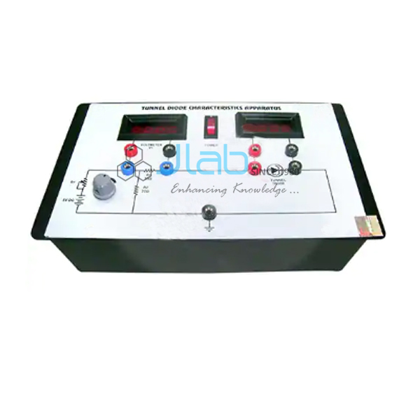
Product Code : EL-DSO-10323
Jlab Export is a leading Tunnel Diode Characteristics Apparatus Manufacturer,and suppliers in India
Tunnel Diode Characteristics Apparatus (code EL-DSO-10323) is an analog electronics lab apparatus for plotting the V–I characteristic and the resistance characteristic of a tunnel diode in forward bias. A fixed +5 V DC regulated supply is built into the unit, which has a Bakelite front panel printed with the symbol diagram. It is made by Jain Laboratory Instruments Pvt Ltd (JLab) at its works in Ambala, India.
Specifications
| Parameter | Detail |
|---|---|
| Objective | V–I characteristic and resistance characteristic of a tunnel diode in forward bias |
| DC regulated power supply | Inbuilt, fixed: +5 V DC |
| Digital panel meter | On board; measures V1 (voltage across resistance R3) and V2 (voltage across the tunnel diode) |
| Current control | Potentiometer R1 |
| Device | Tunnel diode |
| Front panel | Bakelite, 270 x 170 mm, with symbol diagram and all important test points brought out; on a lightweight shock-proof plastic cabinet |
| Power requirement | 230 V AC 10%, 50 Hz |
| Weight | About 1.5 kg |
| Dimensions | 300 (L) x 175 (B) x 75 (H) mm |
| Standard accessories | Power cord, patch cords and instruction manual |
| Quality check | Each apparatus is visually inspected before dispatch |
| Pack quantity | Each (sold individually) |
| Minimum order quantity | 10 units |
| Dispatch time | Usually 7–10 working days |
| Product code | EL-DSO-10323 |
| Manufacturer | Jain Laboratory Instruments Pvt Ltd (JLab) — OEM |
| Country of origin | India (made in Ambala, Haryana) |
What Is the Tunnel Diode Characteristics Apparatus Used For?
A tunnel diode is a very heavily doped PN junction with an extremely thin depletion layer, so electrons can tunnel straight through it. In forward bias its current first rises to a peak, then falls to a valley as the voltage increases further, and finally rises again like an ordinary diode. The falling stretch between peak and valley is a region of negative resistance, which is what lets tunnel diodes work in very fast oscillators and switches. Plotting the V–I curve and the resistance characteristic makes that region visible.
Frequently Asked Questions
What does negative resistance mean here?
Between the peak and valley points the current falls while the voltage rises, so the slope of the curve — the dynamic resistance — is negative. A device with negative resistance can feed energy into a tuned circuit and keep it oscillating.
How is the diode current found?
The digital panel meter reads V1 across the resistance R3; dividing V1 by the value of R3 gives the current, while V2 gives the voltage across the tunnel diode at the same setting.
Why is the characteristic taken in forward bias?
The peak, valley and negative resistance region all appear in forward bias. In reverse bias the heavily doped junction simply conducts, so it shows nothing distinctive.
What information is needed for an export quotation?
Send the number of units, the destination country and port or city, your preferred delivery terms (for example FOB or CIF), any packing or labelling requirements, and a tender reference if there is one.
Who manufactures this apparatus?
Jain Laboratory Instruments Pvt Ltd, trading as JLab, makes it at its works in Ambala, Haryana, and quotes for it directly.
OEM Manufacturer
JLab is the trading name of Jain Laboratory Instruments Pvt Ltd, an electronics and physics lab equipment manufacturer in India, incorporated in 2017 and based on Hargolal Road, Ambala, Haryana. The apparatus comes from JLab’s own works and not from a trader, so schools, colleges, dealers and importers buy from the maker and return to it for repeat orders. JLab exports worldwide and ships to buyers in every region — for example Colombia in South America, Tunisia in North Africa, Moldova in Eastern Europe, Kazakhstan in Central Asia and Hong Kong in East Asia. Tender information is on the JLab lab tenders page.
Related Diode and Semiconductor Apparatus
- PN Junction and Zener Diode Characteristics Apparatus Forward and Reverse V-I Characteristics — for the forward and reverse characteristics of a PN junction diode and a zener diode.
- Voltage Stabilization Characteristics of Zener Diode — for zener voltage stabilization, with load resistances selectable by a band switch.
- Energy Band Gap Apparatus — for reverse saturation current against temperature of a PN junction diode in an electric oven.
- FET Characteristics Apparatus — for the static and transfer characteristics of a field effect transistor.
See also the Semi Conductor Devices range and the Electronics Lab Equipments range.
Request a Quote
Use the Add To Cart button, or send the number of units and where they should be delivered through the contact page.
Last updated: 22 October 2026